A Miniature Multi-Band Antenna for the IoT
Introduction to IoT and Antenna Essentials
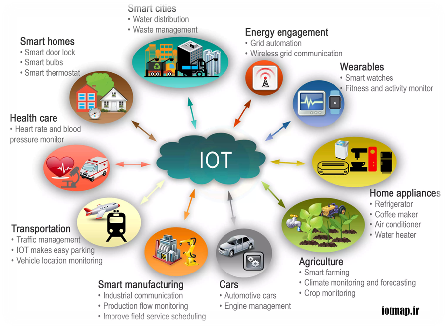
The Internet of Things (IoT) represents a transformative concept where everyday applications and objects gain the ability to communicate and interact over the internet, effectively making "things" more intelligent and interconnected. This vast network of devices brings convenience and efficiency to our fingertips, drastically simplifying daily tasks, optimizing work processes, and offering unparalleled control over various aspects of our lives. At the heart of most IoT devices is the crucial technology of antennas—whether it’s a whip, PCB, or chip antenna—these components are essential for facilitating the seamless connectivity that IoT promises, allowing devices to transmit and receive vital data, thus powering the IoT revolution.
The Challenge of Antenna Design in the IoT Space
In the realm of electromagnetics, size is a critical factor that can complicate the design and optimization of antennas, presenting antenna engineers with significant challenges. For decades, achieving the perfect balance between an antenna's physical dimensions and its performance has been a complex task, often described as a nightmare due to the precision required. The drive towards miniaturization in the IoT sector intensifies these challenges, as engineers must now create antennas that not only fit within increasingly compact devices but also maintain the necessary efficiency, gain, and signal quality. This intricate dance of size versus functionality remains a key hurdle in the advancement of antenna technology.
The Potential of Terahertz Frequencies
One potential solution to the challenge of designing small antennas for IoT devices is to shift to higher frequencies, such as Terahertz. This leap in frequency can significantly reduce the size of antennas required, enabling them to fit within the increasingly compact form factors of modern IoT devices without compromising their performance. While terahertz frequencies offer the potential for smaller antennas and faster data transfer, they also introduce their own set of challenges. One significant issue is the rapid decay of signal strength over distance, compounded by the strong absorption of these frequencies by water molecules in the atmosphere.
Advantages of PCB Antennas
PCB antennas stand out for their efficiency, striking a practical balance between antenna gain and compactness. These antennas are superior to chip antennas when it comes to operating over wider bandwidths while still maintaining high gain. This capability ensures reliable communication over various frequencies, which is vital for the diverse range of applications within the IoT ecosystem. Additionally, the versatility of PCB antennas allows for custom shapes and sizes, making them adaptable to the specific design constraints of a device. They can be finely tuned during the PCB manufacturing process, which can lead to better integration with other circuit components and overall device performance. These factors make PCB antennas a go-to choice for IoT engineers looking to achieve optimal performance without increasing the footprint of the device.
Exploring the Printed Inverted-F PCB Antenna
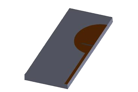
In this application note, we're going to explore the design intricacies and simulation results of a printed inverted-F antenna (IFA), tailored for IoT devices. The antenna we're focusing on is crafted to operate efficiently over the LoRa (915 MHz) and the GPS L1 (1.57 GHz) and L2 (1.23 GHz) bands. This IFA, with its compact dimensions of 40 × 25 × 1 mm³, is engineered on a PCB that uses an FR4 dielectric substrate, characterized by a dielectric constant (r) of 4.3 and a loss tangent (tan ) of 0.025.
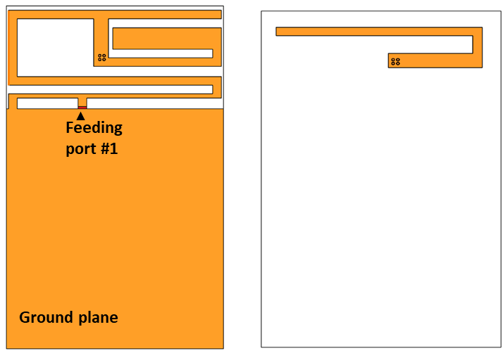
PCB layout top(left) and bottom view.
Our design leverages a meandered IFA pattern to maximize the available space within the limited dimensions. To further optimize space and performance, the antenna utilizes a quartet of vias that allow the meandered structure to extend to the opposite side of the substrate, thereby occupying the back layer as well.
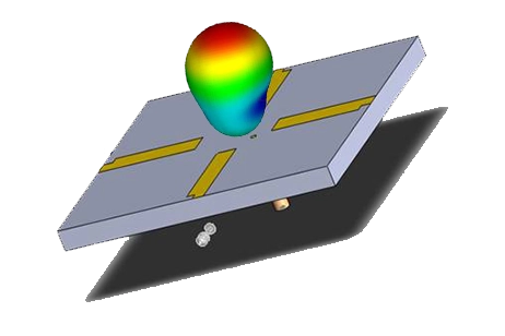
When considering the mobile terminal of an IoT device, we've modeled it as two primary components: the casing and the battery. The casing is imagined as a box composed of a lossless plastic material with a dielectric constant (r) of 2.6, encapsulating the PCB. The battery is modeled to be entirely made of copper, ensuring the model reflects a realistic representation of the terminal's influence on antenna performance.
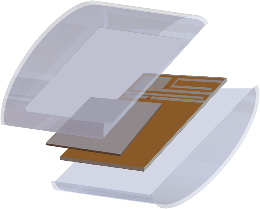
PCB Antenna with Casing and Battery
Simulation Insights and Performance Optimization
Our initial exploration delved into how variations in the strip length
Optimizing the strip length l
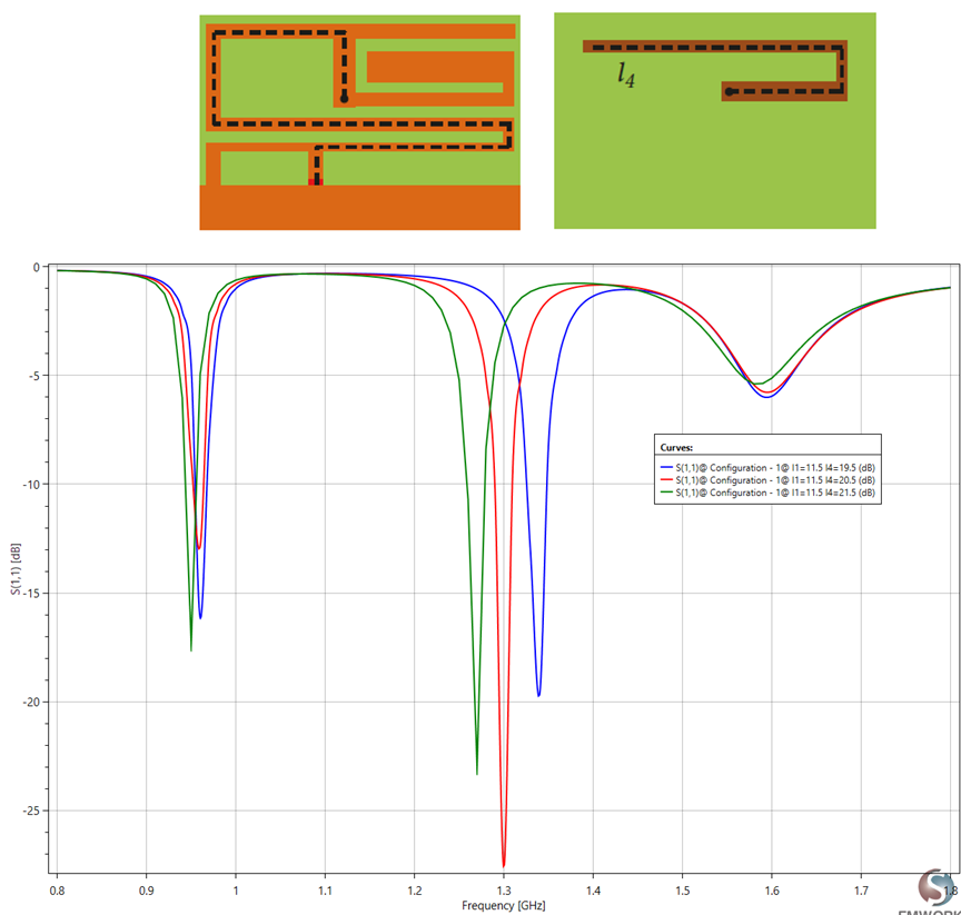
Return loss Vs Frequency for several strip length
Upon observation, it becomes evident that there is a distinct correlation between the strip length of
Optimizing the slot length l

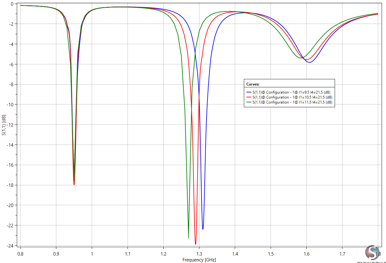
Return loss Vs Frequency for several slot length
Adjusting the slot dimension by manipulating the slot length
Impact of Battery and Casing on VSWR
Subsequently, with the antenna dimensions optimized, we proceeded to examine how the presence of the battery influences the Voltage Standing Wave Ratio (VSWR) of the system. This step is crucial for understanding the interplay between the antenna's electrical performance and the battery's physical attributes, which can significantly affect the antenna's impedance matching and, consequently, the overall efficiency of the radio frequency (RF) pathway.
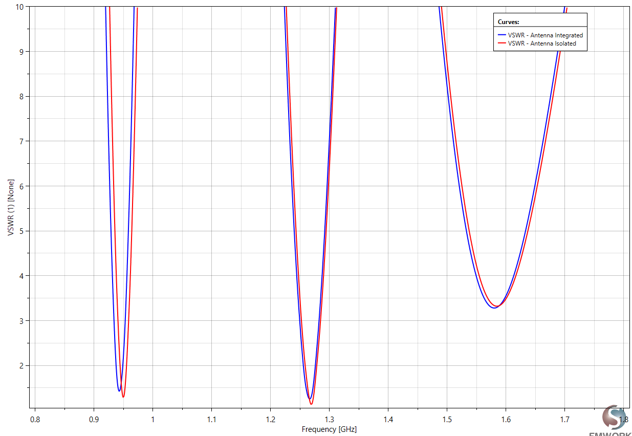
VSWR of the optimized antenna
Observations reveal that when juxtaposed with the scenario where the antenna operates in isolation, the adjacency of other integral device components, such as the battery or the casing, precipitates subtle yet discernible shifts in the resonance points toward lower frequencies. This phenomenon underscores the complex electromagnetic interactions at play within the device's architecture and highlights the need for comprehensive design strategies that consider the close coupling effects between the antenna and its surrounding elements to ensure optimal performance.
Frequency Band Effects on Antenna Efficiency
We proceeded to analyze the impact of different frequency bands on the antenna's efficiency, leading to the discovery of key findings. This investigation allowed us to assess how varying frequency ranges influence the overall performance and energy utilization of the antenna, providing essential insights for optimizing our design for specific applications.
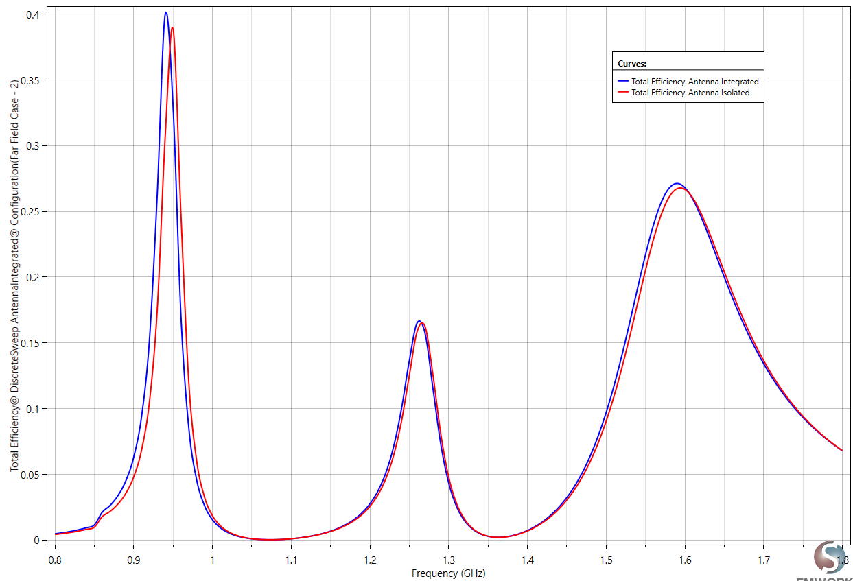
The antenna efficiency Vs frequency
Our analysis revealed that the total efficiency of the antenna varies significantly across different frequency bands. Specifically, the efficiency reaches approximately 40% over the LoRa band, indicating a relatively high performance in this spectrum. In contrast, the efficiency drops to 27.5% within the GPS L1 band and further decreases to 16.5% in the GPS L2 band. These results highlight the challenges of designing antennas that maintain high efficiency across diverse operational frequencies, emphasizing the need for targeted optimizations to enhance performance in lower-efficiency bands.
Gain Pattern
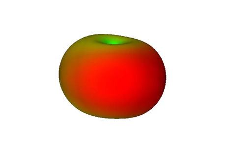
This classical dipole-like radiation pattern makes the PCB antenna especially suitable for IoT applications. Its ability to provide consistent and reliable signal coverage is crucial for devices that require stable connectivity across various environments. Such attributes are ideal for the diverse needs of IoT systems, ensuring efficient communication links essential for the seamless operation of smart devices.
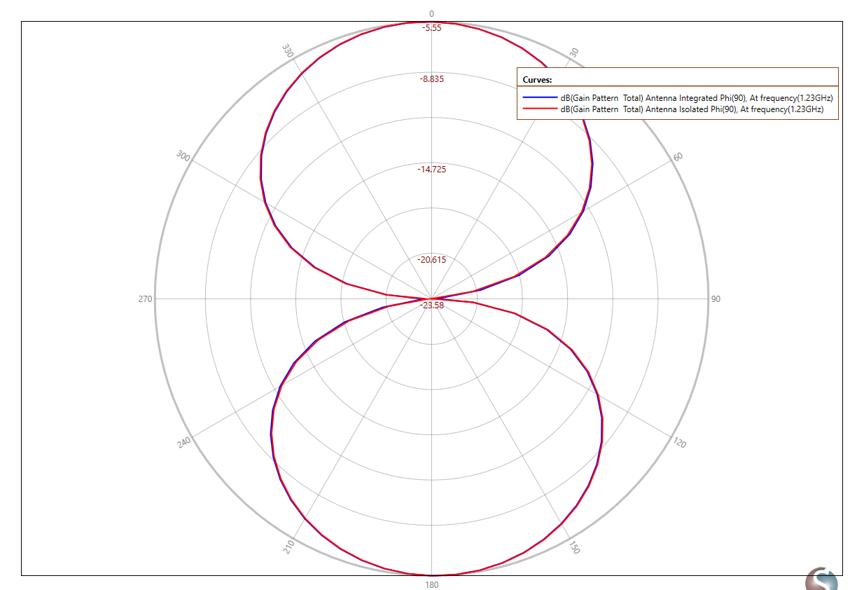
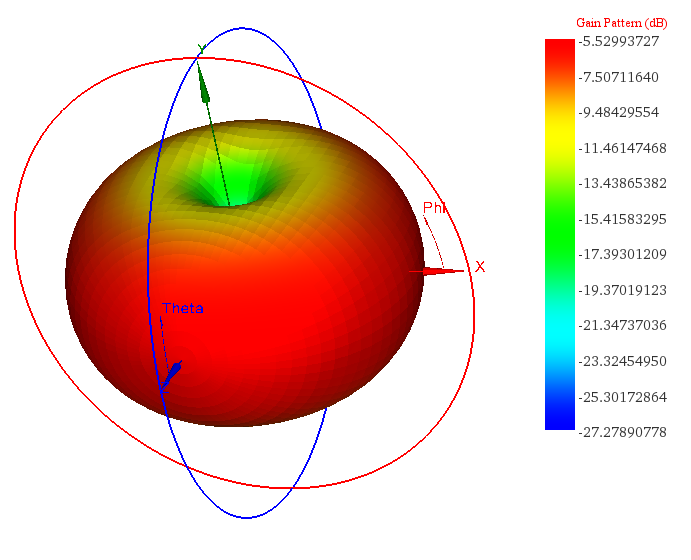
2D Gain pattern at Phi= 90º (at 1.23 GHz) 3D Gain pattern at 1.23 GHz
Conclusion
In conclusion, the development of a miniature multi-band PCB antenna tailored for IoT applications exemplifies the intricate balance between size, performance, and efficiency needed in modern device design. Through detailed simulations and optimizations, we've demonstrated that even within compact dimensions, antennas can achieve substantial efficiency and maintain performance across diverse frequency bands. This exploration into antenna design not only enhances our understanding of electromagnetic interactions but also sets a precedent for future advancements, ensuring that IoT devices continue to evolve with both reliability and precision in their connectivity solutions.


